Charge sensitive preamplifiers (CSPs) are often the best choice when designing readout circuitry for pulse detectors. Their design offers low noise, stability, and their integrating nature provides an output proportional to the total charge flowing from the detector during the pulse event. The gain is stable in comparison to other preamplifier designs: the gain does not depend on the input capacitance or the amplifier bandwidth. It is for these reasons that charge sensitive preamplifiers are usually used in radiation detection applications, where individual detection pulses need to be measured with high precision.
Fundamental Design
The charge sensitive preamplifier design in its most basic 'stripped down' form is shown in the figure below. A feedback capacitor Cf between the input and output stores the charge from the detector, and the gain of the preamplifier is 1/Cf. Each pulse of current from the detector causes the output of the charge sensitive preamplifier to step, the output being the time integral of the detector current. The gain of a CSP is given in units of output volts over input charge (e.g. volts/picocoulomb). Sometimes the gain of a CSP is given in units of output volts per MeV input (e.g. mV/MeV). This assumes the detector made of silicon (which has an ionization rate of 3.6 eV per electron charge) and is detecting gamma rays or energetic particles.
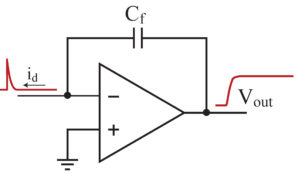
Note that the polarity of the output pulse is positive when the current pulse flows from the CSP input. When the detector current flows into the CSP the output pulse is negative. More on this subject can be found here.
Response to a Detection Event
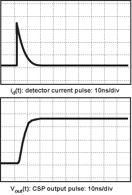
The current pulse from the detector may be collected quickly or slowly, but using the charge sensitive preamplifier design the final preamplifier output remains unaffected by the speed of the charge collection. Thus the response will be unaffected by stray capacitance attached to the preamplifier input or stray resistance between the detector and preamplifier.
An illustrative example of the relationship between the current from the detector and the preamplifier output voltage Vout is shown below:
Modifying the Charge Sensitive Preamplifier Output Response to a Tail Pulse
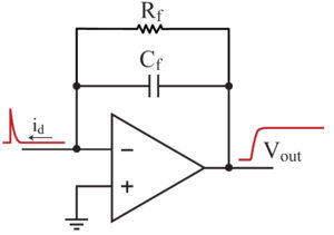
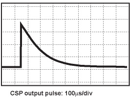
The stripped down charge sensitive preamplifier circuit in the above schematic has no way to be reset - the output will increase until the charge sensitive preamplifier reaches its maximum output. So the circuit as drawn above is not practical. The most common method to reset the charge sensitive preamplifier circuit is to place a high valued bleed resistor in parallel with the feedback capacitor. For Cremat's CR-110 preamplifier, the feedback capacitor value is 1.4pF and the feedback resistor (bleed resistor) is 100 megohms. The pulse response of the CR-110 charge sensitive preamplifier is hence transformed to that of a tail pulse, where the rise time remains as shown in the figure above, but there is now a long decay time as is shown in the figure below. For the CR-110, the decay time constant of the exponential decay is 140 microseconds (1.4pF x 100Mohms).
Shaping the tail pulse into a Gaussian pulse
The output of the charge sensitive preamplifier (with its tail pulse signal shape) should only be considered to be an intermediary step in producing a measurable output. The long tail makes digitizing the pulse heights impractical, because pulses will often ride on top of the long tail of one or perhaps several preceding pulses. To quicken the decay time of the pulses we recommend routing the charge sensitive preamplifier output into a shaping amplifier stage which produces a symmetrical bell-shaped pulse. Another important feature of the shaping amplifier is that much of the noise is filtered, improving the signal to noise ratio considerably. Signals that may be buried in the noise become clearly above the noise after the shaping stage. To illustrate the effect of a shaping amplifier the figure below shows oscilloscope traces of the output an a charge sensitive preamplifier (shown in blue) compared to the same signal after being routed through a shaping amplifier (shown in yellow):
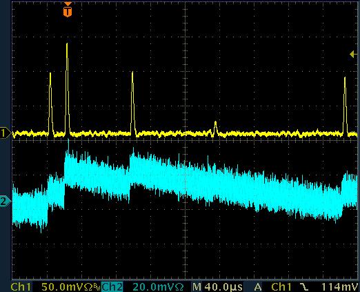
All charge sensitive preamplifier detection circuits should include a shaping stage before the digitization stage, although this shaping can be done in software if the data acquisition setup allows it. An important parameter in the shaping stage is the shaping time, which is proportional to the width of the output pulses. Some guidelines for choosing an optimal shaping time are:
1) Choose a shaping time that will minimize the electronic noise. As was mentioned above, shaping amplifiers are electronic band pass filters - the shaping time is related to the band pass frequency. There are a few sources electronic noise in a typical detection system, and some of them differ in their power spectra. There usually is a 'noise minimum' within the range of available shaping times, meaning that there is a particular shaping time that will filter the most noise. Because changing the shaping time is usually a simple matter of swapping out the installed CR-200-X shaping amplifier module for that of another shaping time, the noise minimum could simply be determined experimentally.
2) Choose a shaping time that is long enough to collect all the charge from the detector. While some detectors can be quite fast, the incoming signal may have a duration lasting microseconds. For example, detection of a light signal from a CsI(Tl) scintillator occurs over a 2 microsecond duration. In this case and in other applications involving relatively slow signals, use a shaping time that is at least as long as the photon signal duration.
3) Choose a shaping time that is short enough to accommodate the expected counting rate of the detection system.
Further reading on this subject can be found in the chapter written by H. Spieler of Lawrence Berkeley Laboratory: Front-End Electronics and Signal Processing.