It is often useful to test the electronics chain in a detection system for proper operation. This is particularly true for the preamplifier, which is a critical stage dictating the overall performance, second only to the detector.
The easiest way to perform this test is by injecting pulses to the preamplifier input with an electronic pulser or waveform generator. However, testing a charge sensitive preamplifier (CSP) is not the same as testing a voltage amplifier where we can simply apply a function generator directly to the input. This article will describe how to make this test using a CSP.
Charge sensitive preamplifiers expect a brief (typically sub-microsecond) pulse of current injected into (or out of) the input. An easy way to apply a charge pulse of known amplitude to the input is by capacitively coupling a square wave generator to the preamplifier input as shown below:
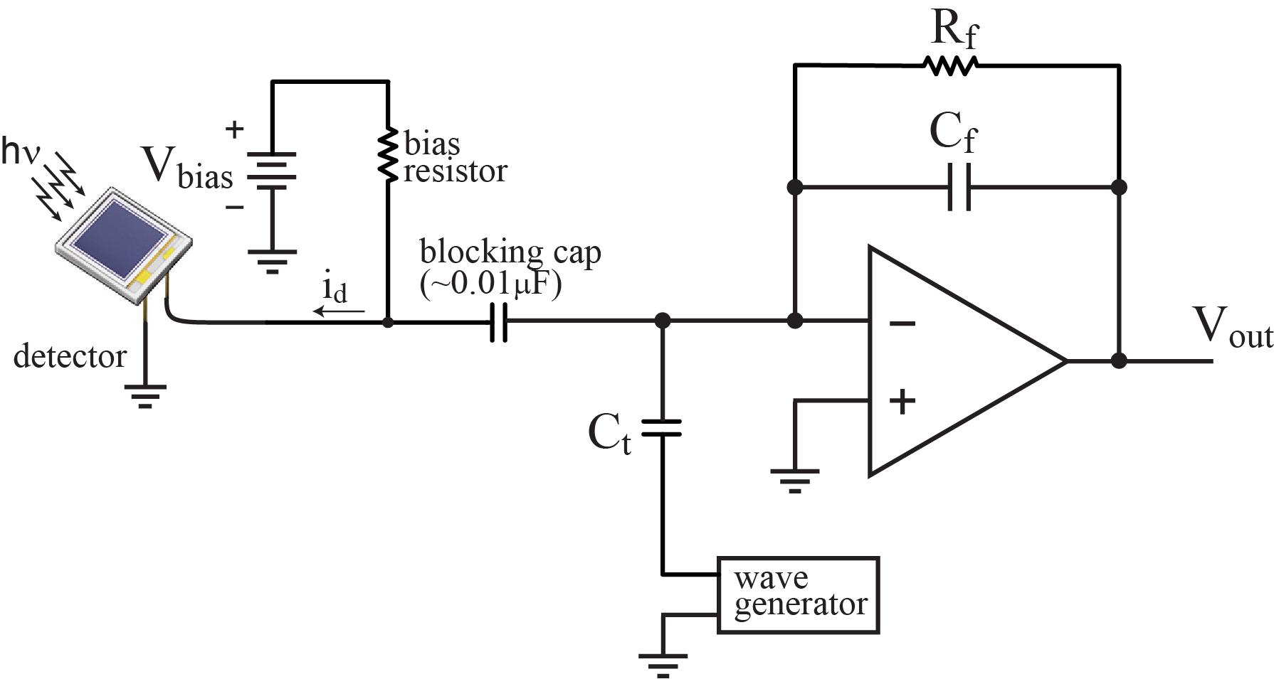
In the diagram above, we see the CSP rendered as an opamp with feedback resistor and feedback capacitor. Also shown is the detector and detector biasing, although this part of the circuit may not be involved in the testing. In fact, we advise disconnecting the detector from the circuit if you wish to test only the CSP.
If you are using the CR-150-R6 evaluation board:
The CR-150-R6 evaluation board already has provisions for Ct as shown above. Ct is C2 on the board. When testing a CR-110 or CR-111, the value of Ct is recommended to be 1pF and is included with the CR-150-R6 board. If testing the CR-112 or CR-113 we recommend using a 10pF value for Ct which is also included with the CR-150-R6 board. The square wave generator shown in the above diagram should be connected to the 'test in' connection on the board.
Applying a square wave using the wave generator shown above, a series of current spikes are applied to the CSP input of alternating polarity. This is shown in the waveforms below:
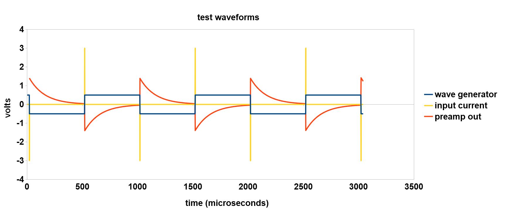
The wave generator in the case shown above provides a 1 kHz 1 volt peak-to-peak square wave (shown in blue). The wave generator is coupled to the CSP input via a test capacitor Ct.
Each time the square wave changes state, a brief current pulse (shown in yellow) is injected into or out of the CSP input through the test capacitor Ct. The amount of charge injected into the preamplifier input is the product of the test capacitance Ct and the peak-to-peak square wave voltage. For example, if the peak-to-peak square wave voltage is 1 volt and Ct is 1 pF, then 1 picocoulomb is injected into the CSP with each change of state.
The gain of the CR-110 CSP is 1.4 volt per picocoulomb, so the CSP output pulse is 1.4 volts (shown in orange). Keep in mind that the output impedance of the CR-110 (and the other three Cremat CSPs) is 50 ohms. So if the oscilloscope termination on the CSP output is also 50 ohms then the gain is cut in half and the output pulse is 0.7 volts.
The gain of the CR-111 CSP is 0.13 volts per picocoulomb, so the output pulse would be considerably smaller (by about a factor of 10) if using this preamplifier. The CR-112 and CR-113 CSPs have even smaller gains, so expect even smaller output pulses if using these preamplifiers. In fact, we suggest using a 10pF test capacitor in place of the 1pF Ct cap suggested earlier to increase the input pulse size so that the output pulse can be clearly measured.
The CR-150-R6 evaluation board is set up so that the test capacitance Ct (C2) can be chosen by installing either the 1pF or 10pF capacitors provided. If using the CR-112 or CR-113 preamplifiers, we suggest using 10pF capacitor, otherwise it is best to use the 1pF capacitor.
The output of the CSP exponentially decays with a time constant given by the product of the feedback components. For the CR-110, which has a feedback resistor of 100 MΩ and a feedback capacitor of 1.4 pF, the decay time constant is 140 μs. This exponential decay is evident in the output waveform shown in orange.
Noise measurement
Measuring the noise can be done in a number of ways. The traditional method requires the use of a pulse height analyzer, which may not be available to many users. For this reason this method will not be described here.
Fortunately, a simpler measurement method exists requiring only modest instrumentation: a calibrated shaping amplifier and an RMS voltage measurement instrument. Many digital oscilloscopes have the capability of measuring RMS voltage which may be sufficient for this purpose. This simpler noise measurement method relies on knowing the gain of both the preamplifier and shaping amplifier and measuring the RMS noise at the output of the shaping amplifier. The equivalent noise charge (ENC) at the CSP input can then be easily calculated. The reason we are adding a shaping amplifier to the output of the preamplifier is that the shaping amplifier acts as a bandpass filter. It is customary in the industry to specify the CSP noise figure as the equivalent noise charge (ENC) at the CSP input when the output is filtered through a shaping amplifier with 1 μs shaping time.
This simple noise measurement will be demonstrated here. The gains of Cremat's CSPs are listed on their respective specification sheets. For this demonstration we will use the CR-110-R2 used within an instrument based on the CR-150-R6 CSP evaluation board used in Configuration 1. Regarding the shaping amplifier, we will use an instrument based on the CR-200-1μs shaping module, CR-210-R0 BLR, CR-160-R9 evaluation board, CR-160-BOX-R9 housing, and CR-24V power supply. The assembly of this instrument is described here.
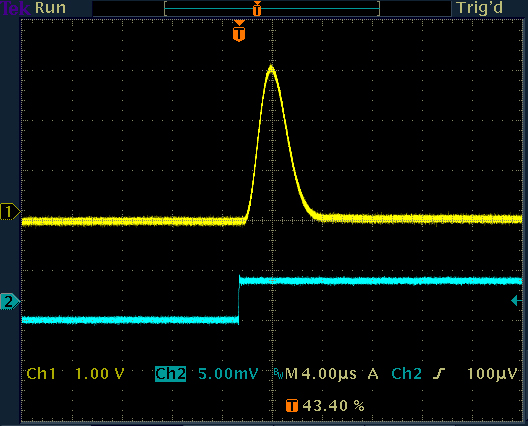
In this demonstration we will rely on the specified gain of the CR-110-R2, which is 1.4 volts per picocoulomb. The shaping amplifier, on the other hand, will be calibrated. To calibrate the assembled shaping amplifier instrument we apply a 4 mV peak-to-peak square wave to the input at 100 Hz. We adjust the coarse gain and fine gain on the CR-160-R9 board to produce a 3 volt Gaussian pulse. The gain of the shaping amplifier is thus 750. The input (blue) and output (yellow) waveforms to the shaping amplifier instrument are shown below:
The overall gain of the CR-110 based CSP and the shaping amplifier is 1.4 volts per picocoulomb x 750 = 1050 volts per picocoulomb = 1.05 volts per femtocoulomb. In terms of electronic charges (=1.6x10⁻¹⁹ coulombs) the gain is 0.17 mV per electron.
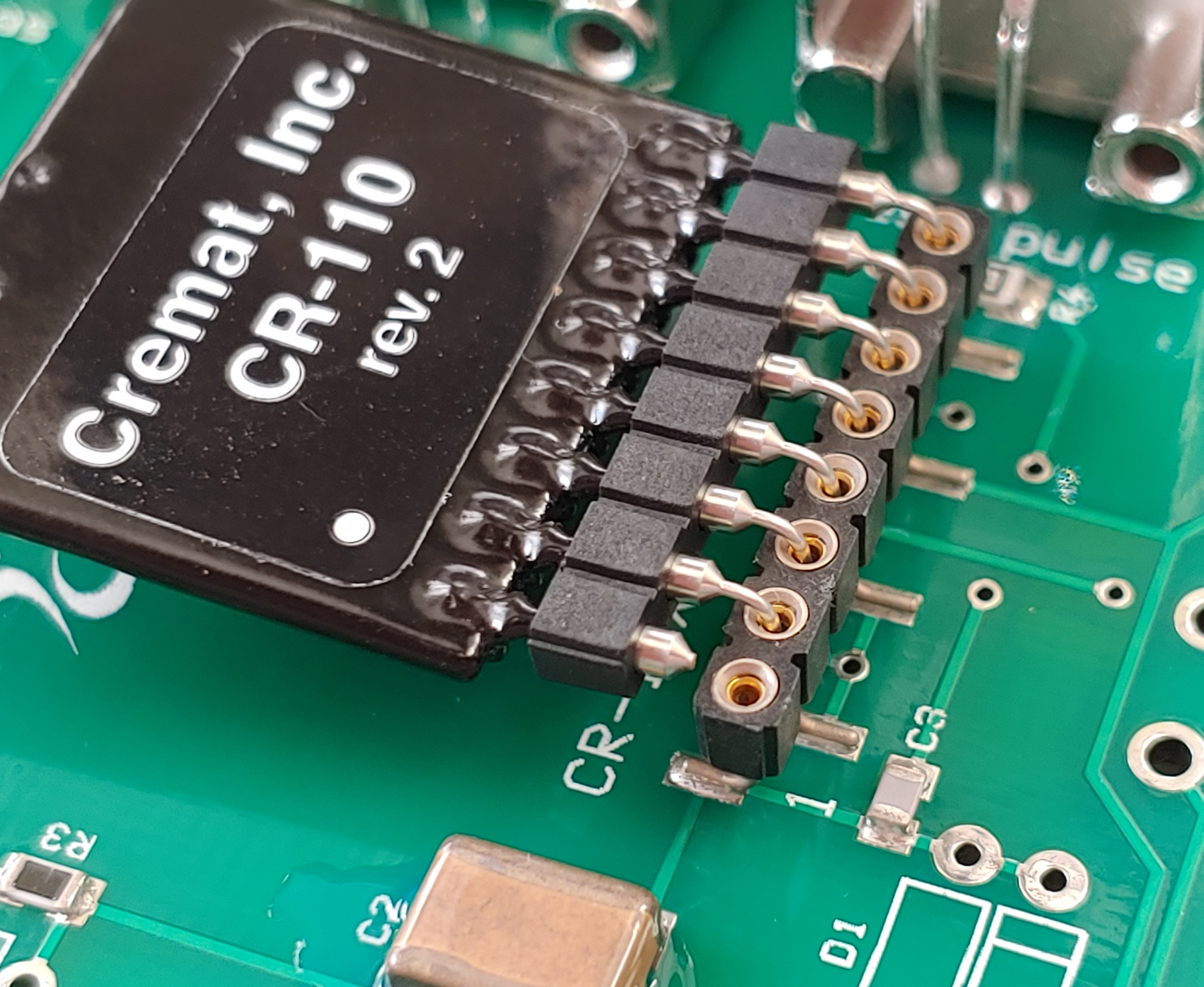
Assuming we are verifying that the CSP is operating within its specified noise limits, we should temporarily lift the input pin (pin 1) of the CSP module from the socket connecting the input node to the main board. This connection to the main board will very likely increase the noise due to a number of factors. Disconnecting the input pin can be done in a variety of ways. In our demonstration we clipped pin 1 of the right angle adapter connecting the CR-110 CSP module to the socket on the main board. A view of the CR-110 CSP with the input pin disconnected to the board is shown here:
Connecting the CSP output to the shaping amplifier, we view the output of the shaping amplifier on an oscilloscope:
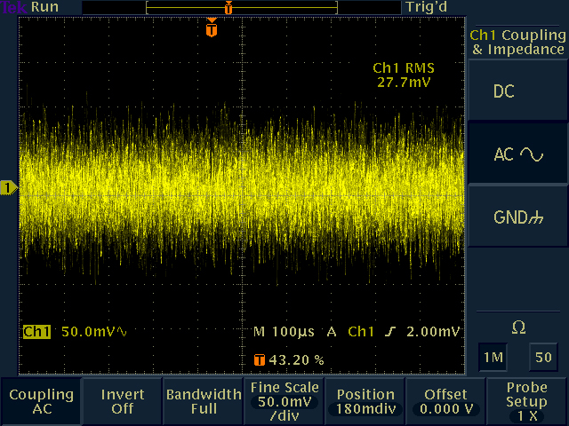
As can be seen, the RMS noise voltage at the shaping amplifier output is approximately 28 mV RMS. To make this measurement accurately, it is important to use "AC coupling" and "1M" input impedance on the scope settings. Otherwise small DC offsets in the shaping amplifier output will add to the measured RMS value.
The equivalent noise charge (ENC) of the CSP is the measured shaping amplifier output noise divided by the overall gain (28 mV divided by 0.17 mV per electron) = 165 electrons RMS.